8085 Microprocessor
8085 Microprocessor
- 8 bit microprocessor
- Introduced by INTEL in 1977
- Use NMOS technology
- The “5” in the model number came from the fact that the 8085 requires only +5V power supply rather than +5V, -5V and +12V as required by 8080 microprocessors.
- It can work up to 5 MHz frequency.
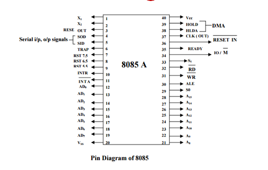
- It has 40 pins.
- Address
Bus : 16 bits
- Can
address up to 216= 65536 bytes (upto 64 Kbytes) AD0-AD15
- Data
bus : 8 bits (D0-D7)
- Program
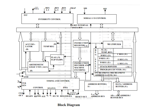
Counter: 16 bits
- Stack
pointer (SP): 16 bits
- Six
8- bit general purpose registers arranged in pairs: BC, DE and HL.
Flag Register
•D4: Auxiliary carry flag•This flag is set to whenever a carry is transferred from D3 to D4, i.e. from lower nibble to higher nibble.•D2: Parity flag•This flag is set to 1 when the result consists of even number of ones.•D1: Carry Flag•This flag is set to 1 when the arithmetic and logical operation results in a carry.
Interrupts in 8085 Microprocessor
•The processor has 5 interrupts which are presented according to their priorities as follows (from lowest to highest):•INTR: It is a maskable interrupt. When the interrupt occurs the processor fetches from the bus one of the 8 RST instructions (RST0- RST7).•The processor saves the current program counter.•RST 5.5 is a maskable interrupt. When this interrupt is received the processor saves the contents of the program counter into stack and branches to 2CH address.
•RST 6.5 is a maskable interrupt. When this
interrupt is received the processor saves the contents of the program counter
into stack and branches to 34H address.
•RST 7.5 When this interrupt is received the processor saves the
contents of the program counter into stack and branches to 3CH address.
•TRAP is a non- maskable
interrupt. When this interrupt is received the processor saves the contents of
the program counter register into stack and branches to 24H address.
Architecture of 8085 Microprocessor
•RESET Signals
•RESET IN: When this signal goes low, the program counter (PC) is set to zero, µP is reset and rests the interrupt enable and HLDA flip flops.•RESET OUT: This signal indicates that the µP is being reset. This signal can be used to reset other devices.•Serial Communication Signals•SID: Serial Input data line: The data on this line is loaded into accumulator bit 7 whenever a RIM instruction is executed.•SOD: Serial Output Data Line: The SIM instruction loads the value of bit 7 of the accumulator into SOD latch if bit 6 of the accumulator is 1.•DMA Signals•HOLD: Indicates that the master is requesting the use of address and data buses.•The CPU, upon receiving the hold request, will relinquish the use of the bus as soon as the completion of the current bus transfer.•Internal processing can continue. The processor can regain the bus only after the HOLD is removed.
•When the HOLD is acknowledged, the Address, Data RD, WR and IO/M lines are 3-stated.
•HLDA: Hold Acknowledge•Indicates that the CPU has received the HOLD request and that it will relinquish the bus in the next clock cycle.
•HLDA goes low after the Hold request is removed. The CPU takes the bus one half-clock cycle after HLDA goes low.•READY:
•This signal Synchronizes the fast CPU and the slow memory, peripherals.


Comments
Post a Comment